Andreas Erdmann studied physics at the Friedrich Schiller University in Jena, where he received a PhD for his work on “Nonlinear optical phase conjugation in photorefractive Bi12GeO20 crystals and applications in optical metrology”. From 1990 to 1995 he worked as a post-doc at the University of Osnabrueck where his research was focused on the modeling of optical waveguides and photonic components based on magneto-optical materials. In 1995 he joined the Fraunhofer Institute for Silicon Technology (ISiT), where he started his work on the modeling of optical lithography for semiconductor fabrication. 1999 he moved to Erlangen to lead the research activities of the “Computational Lithography and Optics” at the Fraunhofer Institute for Integrated Systems and Device Technology (IISB).
In 2010, he completed his habilitation on the “Modeling of advanced mask technologies for optical and EUV lithography”. Since then he teaches also as Privatdozent at FAU. He chaired and co-chaired SPIE conferences on “Optical Microlithography” and “Optical Design” and the International Fraunhofer Lithography Simulation Workshop. In 2016, he was elected as Fellow of SPIE, the international organisation of optics and photonics.
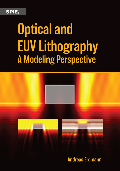
Besides recent publications to e.g. defect detection in lithography masks using deep learning, he published a book on modeling of optical and EUV lithography in 2021.
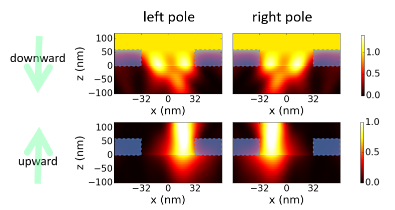
The present focus of the research of our team at Fraunhofer IISB is on the modeling of extreme ultraviolet (EUV) lithography. EUV is the lithography technology for the fabrication of the most advanced microchips. Our group collaborates with ASML, one of the most important tech companies in the world, Zeiss and other partners, to model lithography masks, projection systems and photoresist materials for the next generation of EUV technology. This involves not only an in-depth understanding and modeling of the involved optical and chemical effects, but also the application of deep learning and other machine learning methods to address the extreme computational challenges in this field.
An in-depth understanding as well as accurate and efficient modeling of lithographic techniques become increasingly important for many emerging applications beyond semiconductor technology, especially in the field of design and process technology co-optimization. The close collaboration between designers of semiconductor chips and lithography experts has fundamentally changed both the electronic design of advanced nanoelectronic circuits, and the way how modern semiconductor chips are fabricated. I expect similar developments in other areas like silicon photonics, freeform surfaces for augmented reality virtual reality displays, quantum devices and other applications of nanotechnology.
The combination of FAU, the Max Planck Institute for the Science of Light, two Fraunhofer Institutes, Siemens and smaller institutes and companies makes Erlangen a unique research location with great opportunities for multidisciplinary collaboration and multicultural exchange with students and researchers from all over the world.
In addition, Erlangen has a long-standing tradition in optics. In 1989, few days after the fall of the Berlin wall, Alfred Lohmann (at this time professor at FAU) and Reinhard Voelkel (one of his PhD students) visited the Friedrich-Schiller-Universität Jena, where I just had finished my PhD. During this visit and later meetings with professor Lohmann, I was very impressed by his pioneering work in optical information processing, his extraordinary teaching skills and dedicated mentorship for many students. Professor Lohmann and his students had a profound impact on various areas of applied optics in Germany and beyond.
Use the opportunities to learn about modern optics from different perspectives, find your favorite topic and develop a passion for it. A solid theoretical background, practical research experience from (small) projects and the abilities to explain your research plans and results to others are among the most important things when studying optics and photonics.